Using LBIC as a Tool for Defect Finding and Surface Analysis of Photodetectors and Solar Cells
The LBIC operates by shining a small, focused light beam onto the surface of a solar cell and measuring the resulting current or voltage generated at each point.
This article explores the use of Laser Beam Induced Current (LBIC) as a powerful tool for defect finding and surface analysis of photodetectors and solar cells, focusing on its application in the MADRAS project. While LBIC is a well-established technique in characterizing solar cells, this article aims to demonstrate its practical impact in real-world scenarios—specifically, how LBIC can enhance the development and quality control of printed electronics, particularly organic solar cells and photodetectors integrated into thermoformed or injection-moulded components. By showcasing its effectiveness in identifying defects and optimizing manufacturing processes, this article highlights LBIC’s crucial role in advancing solar cell technologies.
What is Laser Beam Induced Current (LBIC)?
Laser Beam-Induced Current or Light Beam-Induced Current (LBIC) is a technique used to characterize the photo-response of solar cells. In LBIC imaging, a laser beam is focused onto the device to be tested, generating electron-hole pairs within the material at the point being exposed to light. The generated charge carriers then contribute to the power output, which can be measured to evaluate the device's performance. By scanning the laser beam across the device surface, spatial variations in the photo-response can be mapped, providing valuable insights into the device's efficiency and uniformity.
The LBIC generates a detailed digital image of the solar cell, clearly highlighting areas that are functioning properly and those that are not. This allows you to pinpoint defects and trace them back to the manufacturing process, enabling targeted problem-solving and process optimization.
From Technique to Application - A User Case
While LBIC's scientific principles are fascinating, its true potential lies in its applications. One of the standout implementations has been in the MADRAS project, an EU Horizon 2020 initiative aimed at integrating printed electronics into thermoformed and/or injection moulded parts, thus combining the advantages of preparing inexpensive electronics as thin films through roll-to roll processing with the need for shaping and providing integrated functionality to 3D objects. (EU Horizon 2020 No. 862492).
Within the MADRAS project an examination of injection moulded solar cells and photodetectors was carried out by studying the effects of injection moulding on R2R processed organic solar cells.
Flexible organic photodetectors and organic solar cells are, due to their thin profile, inherently susceptible to mechanical damage, necessitating additional protection for certain applications. Traditionally, this protection is achieved by laminating the solar cells into a more rigid panel frame, typically made of glass or plastic, much like conventional silicon solar cells. However, these protection methods can be time-consuming, limit the form factor to flat designs, and result in a bulkier product compared to the thin solar cell foils. This contrasts with the primary objectives for flexible organic electronics, which include rapid production, flexibility, minimal material usage, and low costs.
By integrating thermoforming and injection moulding with the thin structure of organic photodetectors and solar cells, a wide range of applications and new markets can be explored, allowing for the creation of custom-shaped devices. This approach also facilitates a significantly thinner profile than current standards, and depending on the plastic utilized in the injection moulding process, the final product can be either rigid or flexible.
The Light Beam Induced Current (LBIC) technique is an ultrafast imaging method that provides a detailed map of the photodetector’s performance, with each pixel reflecting the efficiency of individual areas - all within seconds to minutes, depending on the device size. By scanning the surface with a high-speed laser, it allows for a resolution of down to 40 µm, making it invaluable for identifying defects and their sources.
-
Like LBIC, photoluminescence is also a powerful technique used for characterizing solar cells, but photoluminescence serves different purposes and provide different types of information compared to LBIC. Photoluminescence is a technique that involves exciting a sample with light and measuring the emitted photons (light) as a result of the sample's recombination of charge carriers. This provides information about the semiconductor's bandgap, recombination processes, and material quality. Photoluminescence is commonly used in the study of the optical and electronic properties of semiconductors, as well as in the detection of defects or impurities within the material. While LBIC focuses on mapping electrical properties and efficiency in solar cell devices, photoluminescence is more concerned with optical and material quality aspects. Both techniques play important roles in the characterization and development of solar cells.
Figure 1: Example of a photodetector with a defective area. Left: picture of the photodetector. Middle: LBIC image of the same cell showing in yellow where the cell is working. Right: 3D image of the photoresponsive areas of the photodetector.
Thin Film Photodetectors for Fingerprint Sensors
One of the core objectives of the MADRAS project is to establish a methodology for injecting moulded organic thin-film photodetectors to be used in fingerprint sensors. During this process, the thin film photodetector is subjected to elevated temperatures while in contact with molten plastics such as polycarbonate (PC), polymethylmethacrylate (PMMA), or thermoplastic polyurethane (TPU). Managing the stress on the multilayered structure — composed of layers ranging from 300 nm to 5 µm in thickness — is vital; The layers must not mix or phase segregate and simultaneously the contact at the interfaces between the layers is essential for functionality for functionality and must not be destroyed.
Figure 2: Architecture of photodetectors prepared on "flextrode" from infinityPV.
LBIC for Analyzing Samples
Analyzing and identifying the causes of any performance degradation due to the injection moulding process is crucial for developing an effective methodology, and LBIC can be a very useful tool in this process. Traditionally, a photodetector or solar cell is characterized by its current-voltage (IV) curve and efficiency, focusing primarily on whether it functions and how its output compares to previous measurements. While this information is crucial, understanding the reasons behind output variations during the development phase is equally important, and LBIC can provide valuable insights in this regard.
Preparation, Injection Moulding, and Analysis of Thin Film Photodetectors
To minimize the thermal effects of injection moulding on organic photodetectors, initial trials were conducted in collaboration between infinityPV (responsible for the photodetector preparation and LBIC) and Eurecat (focusing on injection moulding and electrical characterization). The process is illustrated below:
Figure 3: Step wise procedure for the fabrication of in-moulded organic photodetectors for injection moulding process trials.
Slot-die Coating: Active layers and PEDOT are coated onto “Flextrode,” a flexible PET-based, ITO-free substrate developed by infinityPV, using an RLC sheet coater.
Flexo-Printing: A back electrode is printed with silver-based inks using a RLC sheet coater.
Lamination:To protect the organic photodetector stack, it is laminated with UV-curable adhesives.
Pre-Shaping: The laminated organic photodetector is laser cut into a shape suitable for the selected mould. When the encapsulation material is unsuitable for laser cutting (as with PC), mechanical cutting via a plotter is employed.
Injection Moulding: Various materials such as TPU, PMMA, and PC are used for injection moulding.
Characterization: The injected moulded organic photodetectors are characterized through IV measurements and LBIC.
Conclusion
The integration of LBIC in the MADRAS project underscores its value beyond theoretical principles. LBIC was instrumental in analyzing the impact of the injection moulding process on the organic photodetectors. While IV curves can indicate a drop in efficiency, LBIC can reveal the underlying causes for this change. The combination of both techniques offers a comprehensive understanding of the processes involved. For companies involved in the development of flexible and high-performance photodetectors and solar cells, LBIC thus proves to be an indispensable tool for ensuring product quality and reliability in the fast-evolving field of printed electronics.





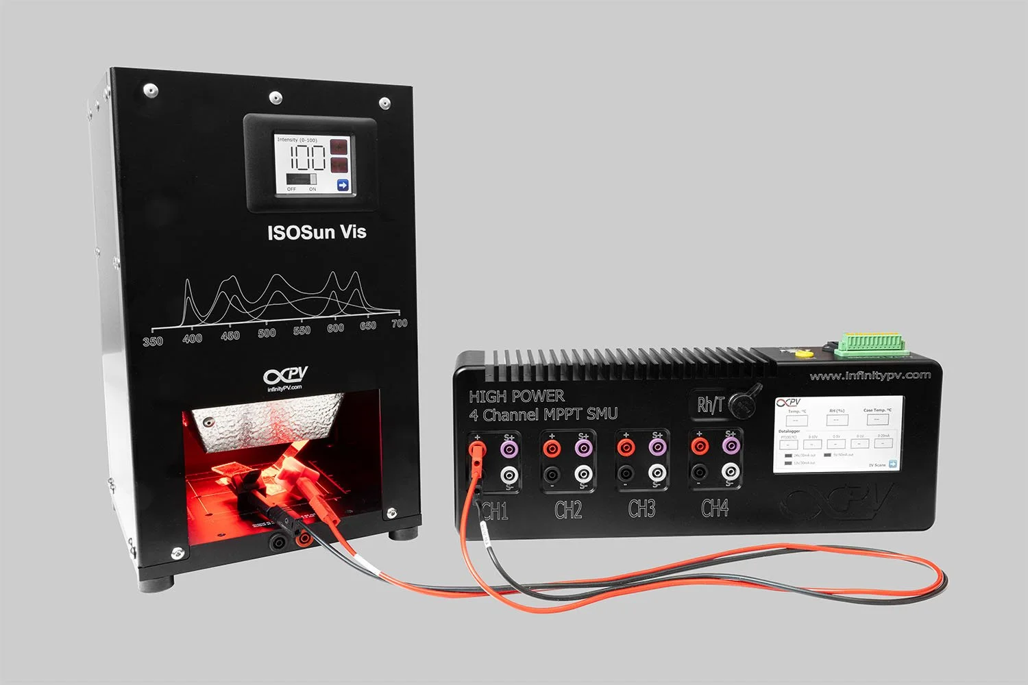
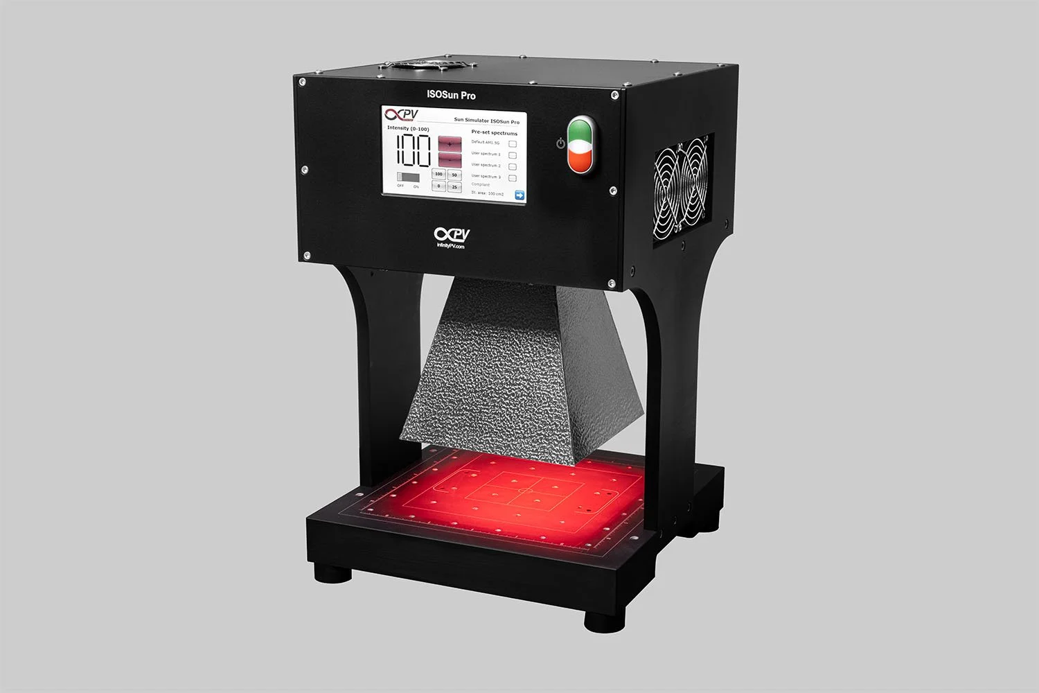
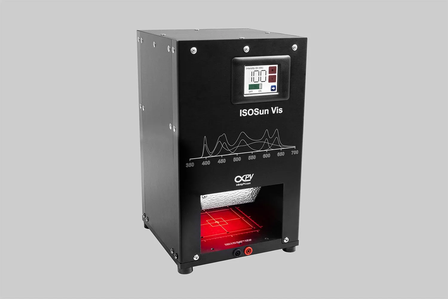
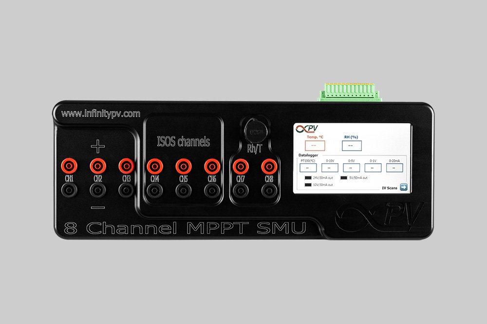




Get started with solar cell research with a complete, ready-to-use system. This bundle combines a compact Solar Simulator and an 8 Channel Source Measure Unit to make PV characterization easy and accessible.